Abstract
I started making my own PCBs at the age of 10, using a pencil on PCB. 10 years later I bought a kit with an UV table, the ferro-chloric acid tank with bubbles and heating, and presensitized copper, but found it very difficult to use for occasional week-end projects and continued to work with the pencil. With SMDs becoming more and more common, pencil is difficult to use for precision work, wasting a lot of time trying to route and adjust PCBs by hand and making marks on the board using needles through paper, which was not great. Over the last 10 years I've been experimenting with various techniques that can significantly shorten the time needed to go from an idea to an actually working board, ideally done the same day for week-end projects. This has now become a reality thanks to two significant improvements: laser engraving and a rocking etching tank. The whole process is described in this article with downloadable schematics and code at the end.

Problems to address and solutions
Over time I've identified multiple problems that needed to be addressed, all of them were causing either long operations or poor quality:- designing: I use pen+paper a lot when thinking. I take notes and draw random circuits regularly everywhere on my paper. But I found that it's very hard to get back to an old drawing for a power supply regulator, a serial converter, a MOSFET driver or anything quite simple that will still waste time redoing. Plus sometimes I'd like to share a schematic with friends, so I started to take photos of some of them and to archive them. Not really convenient. Example:

- testing: using breadboards was nice in the early 2000 but with the trend of SMDs they are less usable or at least you don't as easily transport your circuit from the breadboard to a DIL socket on the PCB anymore. And experimenting with analog circuits is not my favorite thing to do. I'm a programmer and only understand logic. For me an analog signal is a signal that takes a long time to transition between 0 and 1 and has potentially exploitable side effects during this time.
- routing: going from the schematic to the copper traces is a long but relaxing task. Some people play sudoku and others route PCBs. The problem with this is that mistakes are easy to make, and time flies very fast when doing this. It's not uncommon for me to spend 3 hours routing a simple design until it looks usable.
- transfer: the method I was using to switch from paper to PCB relied in simply redrawing the circuit on the copper using a pencil (over the years I developed a pretty accurate mental representation of 1.27 and 2.54 mm pitch that require fairly little adjustment). And when the circuit was a bit too complex then I used to make dots on the copper by picking the paper using a needle. I would then use these marks as start/end points for certain tracks (typically 16-pin DIL circuits). This can also take a lot of time and the result usually isn't great, especially on the edges where connectors are expected to be placed:


- uniform etching: when you put your PCB into the etching bath, if you don't heat it, it can take hours (especially in winter when the solution is cold). And if you don't regularly shake it, the result is often a disaster because locations where the copper started to be removed have saturated the solution with copper, which doesn't act anymore on close places. So you end up over-etching some places and under-etching others. Plus the pencil doesn't help, because it tends to make thin tracks (thus lots of copper removal is needed) and if you try to make large areas they are not uniform in thinkness and result in lots of holes at the end of the etching process. Also the areas where you accidentally put fingers sometimes need to be fixed using a cutter.


- drilling: with all the long process above, it's not uncommon to finally have your etched copper clad in your hands at 2am. And when you're in an appartment, starting to drill at 2am is problematic. Also there's often a missing diameter in your drill bits, not to mention the pain it is to break one at the end of a sunday afternoon when shops are closed.


Without really thinking about these, I actually addressed all these issues one at a time in reverse order:
- I got used to avoid drilling by using SMD components. It turned out that more and more modern components only exist in this flavor. They are way cheaper, do not require drilling nor cutting pins, and result in smaller circuits at the end, which is not bad. Also I found SMD circuits to be easier to adjust in field. Experimenting with different SMD resistor values and changing them in field 4 times is much easier than with PTH (pass-through hole) ones and you much less damage the board. But this has an impact on testing. Making such circuits on breadboard is possible as long as you have equivalent components. This is not always true for some components like micro-USB connectors, large value capacitors, or integrated circuits and you then have to solder one on a small SOP-to-DIL adapter, meaning you have to de-solder later to finally place the circuit on the final PCB, or have another one.


- SMDs being less testable and my difficulties with analog stuff made me naturally migrate to microcontrollers. I've used them quite a bit, even the 8048 and 8051 when I was a kit, which had way too many pins to make clean PCBs by hand (DIL40). But nowadays with Atmel's ATTINY series you can have 1 kB of flash and a 9.6 MHz clock in the size of a 555 for almost the same price, and it requires less components around, resulting in something easier to route!In addition it can be adjusted in field by reprogramming it. That's why I now have a Bus Pirate board with an SOP-8 clamp, to change my mind after the board is finished, and upload program fixes or new EEPROM values.


- excess of etching on SMD ICs causes real mess with too thin tracks or missing IC pads, so I really wanted to address this. In 2010, while patiently shaking a bath during etching, I came up with the idea of making a rocking stand that would do the job for me, which is described below.

- For the transfer, it remained an issue until a few weeks ago when I received my laser engraver, achieving unprecedented results in accuracy and track density.

- however in order to use the laser engraver, it means that I need a digital representation of my PCB and will not perform free-hand drawing anymore. This force me to switch to Eagle CAD. It still is quite a pain for me to use but it finally allows me to archive and share my work, which is not bad, and it allowed me to reach new density levels by removing all the clearance I was used to leave around my components in my free-hand drawings. In the example below, the IC in the middle is not an SOP-8 but a µSOP-8, with a pin pitch of 0.65mm, and as can be seen, there's enough room inside to route up to 4 tracks between the pins!


In the sections below I'll proceed through all these steps to show a workable process for any hobbyist who cannot devote 5 hours on a rainy sunday to try to figure how long to UV-bath a PCB nor to route SMDs by hand.
Designing with Eagle + PCB-GCODE
Interestingly this is the part where I've lost a lot of agility. With pen and paper it can take me 5 minutes to draw an awful circuit that develops the principle I want to realize. But in order to benefit from all the benefits in other steps, you have to give up on pen and paper. In fact not completely.I'm using Eagle CAD for this, which is now part of Autodesk. Its schematic editor is terribly painful to use. It can literally take 2 hours to draw something very simple if you want to do it right, and you very frequently regret having moved something. You can quickly end up with nests of wires all over the schematic that you don't know how to simplify except by destroying them and drawing them again. You frequently "connect" wires to components which are in fact not connected so your circuit is wrong and needs fixing afterwards, and worse, most of the time is spent looking for your component in the library, especially when these are connectors. Except for the nice RLC library which provides standardized resistors, inductors and capacitors, there's nothing like "standard" connectors of various pitches, you have to go through each vendor's catalogue and often end up picking the wrong one. If you take the wrong one and want to replace it later, you'll lose your connections if the pin names differ. In general there's nothing like "generic SOIC-8 circuit" with pins numbered 1 to 8 nor "generic SOT89 transistor" etc. I sometimes ended up giving up after 20 minutes reviewing many components and picking a random one having the same case, even though it results in the wrong part being displayed on the schematic. But the layout is OK (typically a PNP transistor instead of an RF amplifier).

I figured that Eagle CAD really is a professional tool. It's not suited at all to occasional hobbyists because its learning curve is steep and if you use it only every 3 months there's no way you'll use it correctly because you'll have forgotten all its hidden magic. Also recently its license changed. You have to be connected to the net to use it! This is non-sense! The places where I do circuits are exclusively places where I'm away from people and noise, and usually without good if at all connectivity. I understand this choice from a business perspective to fight against piracy and constantly send ads to their free users but quite frankly it totally ruined their product for hobbyists. Thus I'm sticking to version 7.7 which is the last free one and have no intent to even purchase a more recent version which will add more constraints.
Why am I still using Eagle CAD after all this rant, some may ask ? For two reasons. First because the board editor is pretty good even if aging in terms of ergonomy. And the second which is it little secret, because it supports extensions called ULP (User Language Programs), one of which is PCB-GCODE (I'm using the currently latest version 3.6.2.4 found here, as the one linked to from the Autodesk site is outdated). Note that version 3.6.2.4 brings support for stencils which are convenient to make solder masks. Maybe one day I'll try to switch to alternatives like Kicad, but I'll first have to make sure that something equivalent to this extension exists first because this is the key to this tool.
Installing PCB-GCODE on Eagle 7.7
Installing PCB-GCODE is much simpler than I expected. There's a great documentation that comes with it (50 pages, really worth reading), covering in details what needs to be done to install it, and some tricks to use Eagle better. It can be scary at first, but all you need to do is in fact to decompress the archive into your eagle home directory, then go to the Eagle's control panel (the small window that remains open with the list of projects), go to the Options menu, click Directories and prepend "$HOME/eagle/pcb-gcode-3.6.2.4:" in front of the current value:
And that's done! Now from the board editor, when you click on the "Run ULP" icon (the one written in yellow over gray):

It opens a dialog inside the pcb-gcode-3.6.2.4 directory, in which you just have to double-click on "pcb-gcode-setup.ulp" to launch it:

Contrary to my initial impression this is not the installation utility but the utility you run to set up your work (step between passes, layers etc:

This is where you can choose which layer(s) to generate the outline for, the minimum clearance you want between any track, the maximum one as well (since adding clearance passes takes time), and the step size, which is the amount of material removed on each pass. We'll see this below. For now all you know is that PCB-GCODE is properly installed and that you can start to use Eagle to draw your schematic.
Creating your circuit
You will spend some time here, so if you want to parallelize your work, have a look at the section on painting the PCB below so that you can launch that operation and let it dry while you're drawing the PCB.You just have to create a new project, it will open the schematic editor. In this one you add components by picking parts from the libraries (or download other libraries from the net), draw wires between them and your schematic is done. It's very important to systematically move your components around after attaching a wire, to make sure the wire is really attached. It's not because it touches that it is attached. When you move your component around you'll see the wires move with it, confirming the operation. I noticed that sometimes the link was established by moving the component:

Once the circuit is finished, switch to the board editor, place your components, either route manually or using the autorouter (I personally try a combination of both, start with the autorouter then fix what I don't like). It's important to place the components on the correct side, and with SMDs it's easy to get them wrong. While I find more natural to work seeing the top, I'd say this works fine if you exclusively use SMDs. If you mix SMDs and PTH components or just connectors, better keep the top for PTH and the bottom for SMDs (and try to get trained to seeing through the PCB because then all your components are reversed). To switch a part to the other side, just mirror it. Pads appear on both sides from what I've seen. I haven't figured yet the best practice to shrink the board's size once the traces are drawn. Maybe it's better to always keep the same amount of clearance everywhere to get a reference, maybe better align it to the closest track while still respecting DRC rules, I don't know. Typically you'll get this result (note that I did it on the wrong side again, the red one is the top):

Generating the outline for copper tracks
Now's the moment to convert this to the operations needed to turn around the tracks to make some clearance in small steps. We'll call pcb-gcode-setup again and configure it to emit an outline for the relevant side (theorically bottom, but top in this example). Then it's needed to configure the step size and the minimum and maximum amount of clearance around the tracks. This requires a bit of background.With a laser, the spot is very thin and is not round. It's more like the intersection of two ovoids which are almost rectangular. When one dimension is thin, and bright, the other one is not focused and conversely, so when you adjust the focus to see the smallest spot, you have something between a round and a square, with most of the light concentrated into a small spot. The quick drawing below tries to explain this better.

The most concentrated adjustment above (the middle one) will show the highest power density at its center, still with an effect, albeit smaller, when touching the two ovoids of the axis (axis of the laser diode, unrelated to the engraver's so you don't even choose). So even if to the protected eye it appears like half a millimeter wide dot, in practice the active area is way smaller and will require numerous passes with very small steps in between. Also, the energy spread by the two avoids will definitely affect some tracks' shapes during these passes. This is usually visible around very small round pads which end up not being exactly round and are slightly larger on an axis than the other one depending on the initial beam inclination.
But this is not a problem at all once well understood. In my case I tried with 0.05mm between two passes and that was not enough, sometimes a few very thin remains of copper still appeared (less than 0.05mm wide), as can be seen below. Note that it's barely visible to the naked eye, you need a magnifier or a microscope to detect these anomalies (I'm using my camera which has a resolution of ~0.01mm) :

The integrated circuit pads are roughly 0.35mm wide and the space in between is about 0.3mm. The steps were too large (0.05mm) and the beam was not wide enough to erase 0.05mm of matter at once. Thus I'm using 0.025mm passes and up to 0.6mm clearance, which leads to up to 24 passes! Note that my engraver uses 80 steps per millimeter so in theory it is able to move the beam in 0.0125mm steps (12.5 microns).
In practice after setting the passes to 0.025 or even lower, occasionally a very thin line will remain. It turns out that micro-stepping (the principle of moving a motor of less than one step) isn't always perfectly precise and that some very small areas may sometimes be missed. This completely disappeared after I upgraded my motor drivers for more accurate ones, I'll explain this in another article. But even then, such very thin tracks are harmless and are so thin they can be removed with a soft but sharp blade if needed.
In the second tab ("Machine") it's possible to adjust the feed speed, which is the speed at which the head moves when the laser is on. I used feed speeds of around 380 mm/minute but my engraver was calibrated at only 25% power (max of 1000 while I produced files using a power of 255). I successfully used about 1200 since then but that was after changing the motor drivers, so you need to experiment there. You can start with a low value for a small PCB to get an idea of the time it takes and if it gives a good result in a reasonable time, no need to further optimize.
Once the settings are filled in the boxes, just click on the "Accept and make by board" button. Then the board editor appears again with some automatic processing inside it. The layer is first filled, then cleared around the tracks. It will take a few seconds to a few tens of seconds depending on the number of passes and the board's size. The progress is visible in real time with each pass causing the screen to be updated:

It's worth noting that with too small boards, the software ignores the board's size and takes some margins around. I haven't yet figured exactly what's happening, I've suspected it could be due to the device names which cause some text to artificially expand the work area, as visible above with "TINY13V" stretching the area, but I could be wrong. Once the process is complete, the resulting work is previewed for each side and output:

It's possible to remove the colors (C) zoom (+/-), move (arrows) or quit (Q). Each colored line corresponds to a different pass. Note above that the margin is huge and the reported board size was definitely affected by this centering issue that I suspect to be caused by the text. For now I've dealt with this manually by post-processing the G-CODE output. The files are in the project directory with extension ".tap". G-CODE is pure text so they can be consulted and even modified with any text editor.
Due to the way the tracks were made in incremental steps, it results in numerous laser head moves which tend to take a lot of time. There are many G-CODE optimizers available on the net, some directly running into the browser. These ones are useful in that they'll apply some optimization algorithms which reduce the head's travel time. In practice most of the time they will result in making all passes around a given track (or set of tracks) before going to another track. In my experience it can roughly cut the engraving time in half. That can be 30 minutes of work saved for 30 seconds of optimization so it's worth trying. I've successfully used the one on xyzbots.com though it requires a bit of care because sometimes it doesn't update its contents if it detects an error, and renders the previous one instead.
Preparing a copper clad
Now that we've addressed the design and routing parts of the job, we'll have to work on the transfer from the file to the board. When I was experimenting with various methods several years ago, I had the idea of using a UV laser diode to selectively lit a presensitized copper clad and replace the transfer paper and the laser printer approach that almost always gave me poor results. And while thinking about this, I thought "ah if at least we could have a powerful enough laser to directly burn the protective layer, we'd save so much time and steps, thus reducing the cumulated quality loss. Obviously when I saw this inexpensive laser engraver, I thought it would be a real failure from me not to try this old idea.I considered a few approaches for the protective layer:
- paint
- solid ink
- tape
I could run some tests on electrical tape and a few other plastic tapes like the thin brown one for use with cardboard boxes. The laser properly destroys the matter there, but the result is dirty and messy because there is still some glue below the burnt tape and when you try to remove it, you tend to make other parts move. Note, I think it is technically feasible this way with a lot of patience, but in my opinion it's not worth it.
I went to a local DIY store to buy a spray of black mate paint. I wanted the blackest possible and really mate so that it would absorb the maximum amount of light and would not require to work at too low a speed. Well, to make a long story short, at this point I have not found anything better. There are multiple benefits in using paint:
- it's easy to store, just keep the spray bottle, it's always ready for use
- it's relatively inexpensive (~8 EUR for ~300mL I seem to remember)
- it's quite fast, they indicate 30mn before touching but in practice when it's hot and dry enough in 5mn it's usable.
- if you're not happy with the result, just clean it up and do it again.
- the paint layer is extremely thin thus the etching precision is not affected too much and the result is ultra-precise:

- there is a single material in all the depth, contrary to tape which has plastic (or paper) on top and glue at the bottom, so the cleaning is much easier.

Since then I found better than going outside, I just place a large piece of paper on the ground and put the clad on it before spraying. This way I can leave it unattended while it dries. You must just be careful not to have too much dust in the air which can deposit on it, nor to walk too close.


Now it's time to place the painted clad under the laser head, adjust the focus so that the dot is barely visible with the glasses, that's when it's the thinnest and has the most absorption by the paint, and send the G-CODE there. I found that if the surface on which the PCB is placed is not perfectly stable or risks to vibrate during the moves, it's sufficient to place some wet absorbing paper or toilet paper under the board to keep it firmly in place.

Engraving the circuit outline
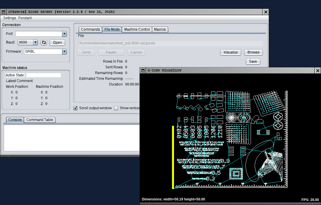
The G-CODE sender I'm using is UGS classic and it works well enough for this job, and shows the progress made, which is appreciable. It requires Java 1.8 but doesn't have any extra dependency. It worked out of the box on my Slackware. What's nice with paint is that you don't destroy any hardware (except the paint itself) during the tests, so you can actually try to send your file there, observe the result, and try again with different parameters if desired, or even try different G-CODE senders.

You will note above that the PCB does not start at the origin and leaves a lot of unused margin, which I really do not want. This is where I'm using my gcode-fixup utility to measure the work area, and apply a compensation offset to X and Y:
$ gcode-fixup laserdot.top.etch.tap | tail -n1
(minx=3.584800 miny=13.376500 minz=0.100000 maxx=26.330500 maxy=25.688700 maxz=0.100000 maxs=0)
$ gcode-fixup -X -3.5848 -Y -13.3765 laserdot.top.etch.tap > top.gcode
$ tail -n1 top.gcode
(minx=0.000000 miny=0.000000 minz=0.100000 maxx=22.745700 maxy=12.312200 maxz=0.100000 maxs=0)
And now by using this file it's properly aligned and starts exactly on the edge, so I can align the laser dot to what I want to be the lowest corner in terms of etching:

Now's time to release test button on the laser module, the put one's protection goggles and to the Send button in the interface and see the work being done.


There is very little smoke on this paint and it smells like acrylic. So it might actually be made of tiny acrylic grains which then burn without residue. The traces appear pretty clearly when lit under a strong light while it is engraving (keep your protection goggles on even if you don't feel that the beam is blinding). After two minutes or so, the work is complete. The paint is burnt around traces for at least as large as configured (typically 0.025 to 0.6mm). The copper may be revealed in some areas when the paint was cleanly vaporized. Let's pass this under tap water to clean the residue. I scrub it with a toothbrush. It's possible to press moderately strongly, the paint is resistant. Pretty quickly all the burnt paint disappears and reveals a pretty precise copper track.

At first this is a bit confusing because you're seeing copper where there won't be any at the end of the process. Just keep thinking that the paint works like the PCB pencil or some transfer paper. Note that the copper is not that clean above because the steel wool I had was very thick and was leaving many scratches. Since then I bought a much finer one which leaves a mirror-like copper clad. Do not put your fingers on the copper yet, it's still sensitive to fat.
Now mission accomplished, we've got a computer assisted schematic transferred very accurately to the copper clad. The rest of the process is well known and more straightforward. Except if we like to have a bit of fantasy...
Uniform etching
Remember the horror stories with stagnant ferro-chloric acid etching different areas at different speeds above ? In 2011 I tried to address this issue by making a rocking stand to place the etching tank, with the PCB in it. For this I reused a servo I had (one with a broken gear exactly in the middle, which I replaced in a robot). I fixed it to a plexiglass plate with rubber pads to prevent slipping and made a circuit to produce oscillating pulse width to make it oscillate left and right. The construction is not particularly solid, just using two screws on one side to rock it and a single screw on the other side to serve as an axis, but it's OK since it never has to take much weight. I've added a mobile LED strip that I directly connect to an external battery to send some light from below and see how the etching progresses, as the epoxy is translucent and thus heavily contrasts with the remaining copper areas. It looked like this (and I still use it for each and every PCB I make):


By then the circuit was tailored around a PIC 12F675 micro-controller which was programmed in assembly. It took quite some time to experiment with various oscillating patterns because each time the program had to be rewritten differently.
The first attempt I made was a naive triangle wave, like the following, consisting in simply doubling the speed compared to the time and inverting the direction at mid-trip. This repeats when reaching a full period:


But looking at the curves above, it's worth ignoring the repetition and starting to look closer, particularly at the shape of the part between 0.75 and 1.

Doesn't this curve remind you something ? It looked to me like a parabola. And this didn't surprise me, I had some very old memories of math lessons seeing how trigonometric functions were calculated using polynomial functions with declining ratios as powers were increasing so it made sense that the square was dominant somewhere in the curve. I compared it with the parabola from a normal square function scaled to the same range:


This ends up like this (using floats and a period of 1.0, directly usable in gnuplot):
 frac(x) = x-int(x)

 sq(x) = x*x

 sin2(x) = x>=0.75 ? sq((x-0.75)*4)-1 : x>=0.5 ? sq((0.75-x)*4)-1 : x>=0.25 ? 1-sq((x-0.25)*4) : 1-sq((x-0.25)*4)
Let's zoom on the first period on the two functions now:

I measured no more than 6% error in the worst case in the middle of the curve between the two when using 8-bit integers for my variant. That was perfect for my use case. And since I already had implemented the 8*8bit multiply to handle scaling, I didn't have much more to implement there.
Now given that we don't care about the sine value but only about respecting the repeating pattern, we can shift this by half a period, use a period of 256 steps, and use the most significant bit of the input as a sign bit for the result after the multiply. This has the benefit of resulting in very small code, and looping on the counter overflow. The algorithm is so simple that it was reasonably easy to redesign it for an AVR micro-controller programmed in C:
/* returns ((x*x) >> 7) + 128 using exclusively a 8*8=>16 bit signed
 * multiply. AVR: ~0x18 bytes + call to mulhi3().
 */
uint8_t sq8(signed char x)
{
        x += 128;
        x = ((int16_t)x * x) >> 7;
        return ~x;
}

/* returns sin(angle*pi/128)*128, which is a sine centered around 0. */
int8_t sin8(uint8_t angle)
{
        uint8_t ret = sq8(angle << 1);

        if (angle & 128)
                ret = ~ret;
        return ret + 128;
}
A PCB was made, taking into account the lessons learned from the 12F675 version. First it uses the exact same footprint as the previous board to support replacing it. Second, while the previous version had a jumper to use only the first half of the servo's range to support my servo with a broken gear, I figured it was still not convenient to perfectly center the stand, so instead this jumper was replaced with a 3rd potentiometer to center the stand. The 3 potentiometers are thus:
- center: defines the location of the zero (more exactly the base value added to the pulse width).
- range: defines how far the stand goes in each direction around the defined center.
- speed: defines how fast the stand moves.
And now look below how a circuit being etched bounces back and forth and is uniformly caressed by the acid. The light that comes from blow is emitted by the LED strip visible above. One day I should think about removing that annoying sticker under the tank.
The final circuit looks like below and can be downloaded along with the code and pre-compiled firmwares for ATTINY13 and ATTINY85 on GitHub here.


What I usually do is to put some ferro-chloric acid in the tank, place this in the microwave oven for 20-30 seconds and heat it to about 50-60 degrees C. That's the temperature where I find it the most effective. Then I throw the PCB into it, and in less than 5 minutes it's finished and perfect. Here is what it looks like for the circuit featured above, first just after rinsing it under clear water, then after removing the paint using steel wool:


One benefit of this etching method involving the laser making contours around the traces is that it removes little copper, is fast to etch and does not consume the acid too quickly (I probably only reloaded mine once over the last 5 years). However there is quite a visible problem here: the outer track remains and while it will usually not be a problem it can become one if some connectors have to be placed flat over the board (which is what this circuit will experience). This is extremely rare, but if this happens you have to pull off the outer copper track using a sharp knife.
Adding a solder mask
Why not add a solder mask ? It's really superficial and not a requirement but it can actually protect the tracks from corrosion and give a cleaner finish to the board. I experimented a bit with a sheet that is supposed to be processed using UV light. It's a thin layer of resin between two thin plastic foils. The two methods I've attempted for now are a bit dirty.In the first cases, I'm using the stencil output from PCB-GCODE. It contains all the SMD components pads. I directly send it using UGS and cut the pieces through the top plastic layer. It's important to know that the blurry side needs to be etched mirrored and the other one has to be etched normally. In order to limit the number of mistakes, I first etch a piece of cardboard and if I'm satisfied, I then switch to the real solder mask.

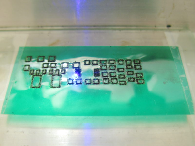

But I found that, as expected, the stencil is made for the solder paste so it doesn't include pads for some connectors. I will have to see in the PCB-GCODE extension if it's possible to enforce the use of extra layers to force these ones to appear.
Hence the second method, for use when some pads are missing. I tried different approaches, one involving a PDF export and pdf2svg (which gave me very poor results because there were inner and outer paths for each pad). The other one was different, in Eagle I performed an EPS export using the CAM processor, enabling only the tCream and Pads layers. I then imported the EPS file into Inkscape, it respects original dimensions and has the exact same drawing. At this point it is possible to proceed in raster mode using 305-Engineering's extension. At 10 pixels per millimeter the output is reasonably quite clean.
However in both cases it appears that the green foil is extremely reactive to heating, so it's important to only cut a small piece. During the cut you can hear some loud pops. And the raster mode is way more straining for the matter, so I wouldn't exclude to see it catch fire one day. Thus it's important to be careful.

Another point to keep in mind is that the laser's wave length is close to the UV used by the resin to polymerize and harden. So I don't know if it can work fine for large surfaces, maybe some parts will harden while other areas are being cut. This needs a bit more experimentation.
Once cut, just use the toothbrush to remove the burnt parts. Use two pieces of duct tape pressing the plastic in sandwich and placed against each other, and pull them off. The blurry side will be peeled off without damaging the green resin. You then have to place it on top of the PCB and be careful to properly adjust it until all pads are correctly exposed. The green resin is slightly sticky so once pressed it will stay in place. But do not abuse this property, the resin is extremely fragile and will break if pulled more than 3 or 4 times.


The wise reader will note that I forgot to peel off the outer copper track on both circuits above one. For the resin to properly attach to the copper, it needs to be laminated or at least heated and firmly pressed. I don't have a laminator so instead I used a thick copper plate and a heat gun for 1 minute at around 100 degrees.

Note that I forgot this step for the circuit on the left and the difference will be visible.
The resin now needs to be exposed to UV light for 30 minutes approximately before the top plastic layer can in turn be removed. The UV lamps normally used to transfer PCBs are perfect for this. The plastic protection must not be removed yet. I did this mistake for the board on the right:


Beware that the board will be very hot at the end and will slightly stick to the glass. As long as it's only the plastic which sticks it's not dramatic though, but I slightly damaged the other one which didn't have its protection anymore. I haven't found a solution to this yet, but it's not a big deal. After this you can use either some duct tape or a sharp knife to peel off the plastic and reveal the solidified resin. The one which was not heated didn't stick well and lost some parts when doing this. The other one is perfect.


Last step, tinning the exposed areas
Once the board is protected with its solder mask, it's possible to bath it into a "liquid tin" solution (in fact it's a mixture of tin sulfate and I don't know what else to reduce the redox potenial). One minute is more than enough, in fact in a few seconds the exposed pads already become silvery:
I'm personally not convinced by this operation. The few times I did it I found that the solders were more difficult to take than with raw copper. Maybe it protects better over the long term, I don't know. Potentially we'd need a similar solution for gold plating, but it must be quite expensive. I'll probably try this again a few more times and will give up if I see that the results make the soldering operation more difficult.
Conclusion
This process looks long here but it really is not. The longest part is to draw the schematic. I think that I'll end up making my own library of generic devices to save a lot of time.The solder mask looks great but I don't know if it really brings any benefit. It adds to the time needed to finish the circuit, and also makes it more difficult to debug it if it does not work. However when properly done with effective separation between pads, it avoids accidental solders between very small pins, so it might be worth using if soldering some PLCC48 for example.
It allows to make impressively clean PCBs with components that I never imagined I would one day be able to use (such as µSOP-8 with 0.65mm pitch), and this the same day as the idea happened, which is unprecedented for me.
Links
- Laser Engraver: https://www.banggood.com/2500mW-A3-30x40cm-Desktop-DIY-Violet-Laser-Engraver-Picture-CNC-Printer-Assembling-Kits-p-1003863.html?cur_warehouse=CN
- Eagle CAD: https://www.autodesk.com/products/eagle/free-download
- PCB-GCODE: https://groups.io/g/pcbgcode/files/2Software/pcb-gcode-3.6.2.4.zip
- G-Code optimizer: https://xyzbots.com:4000/gcode-optimizer/
- Universal G-Code Sender: https://winder.github.io/ugs_website/
- g-code fixup and manipulation utilities: https://github.com/wtarreau/gcode-fixup
- code and circuit for the rocking stand: https://github.com/wtarreau/rocking-stand
- Bus Pirate board: http://dangerousprototypes.com/docs/Bus_Pirate